
3D-Printed Ceramic Robotic Arm: A Breakthrough in Chip Manufacturing
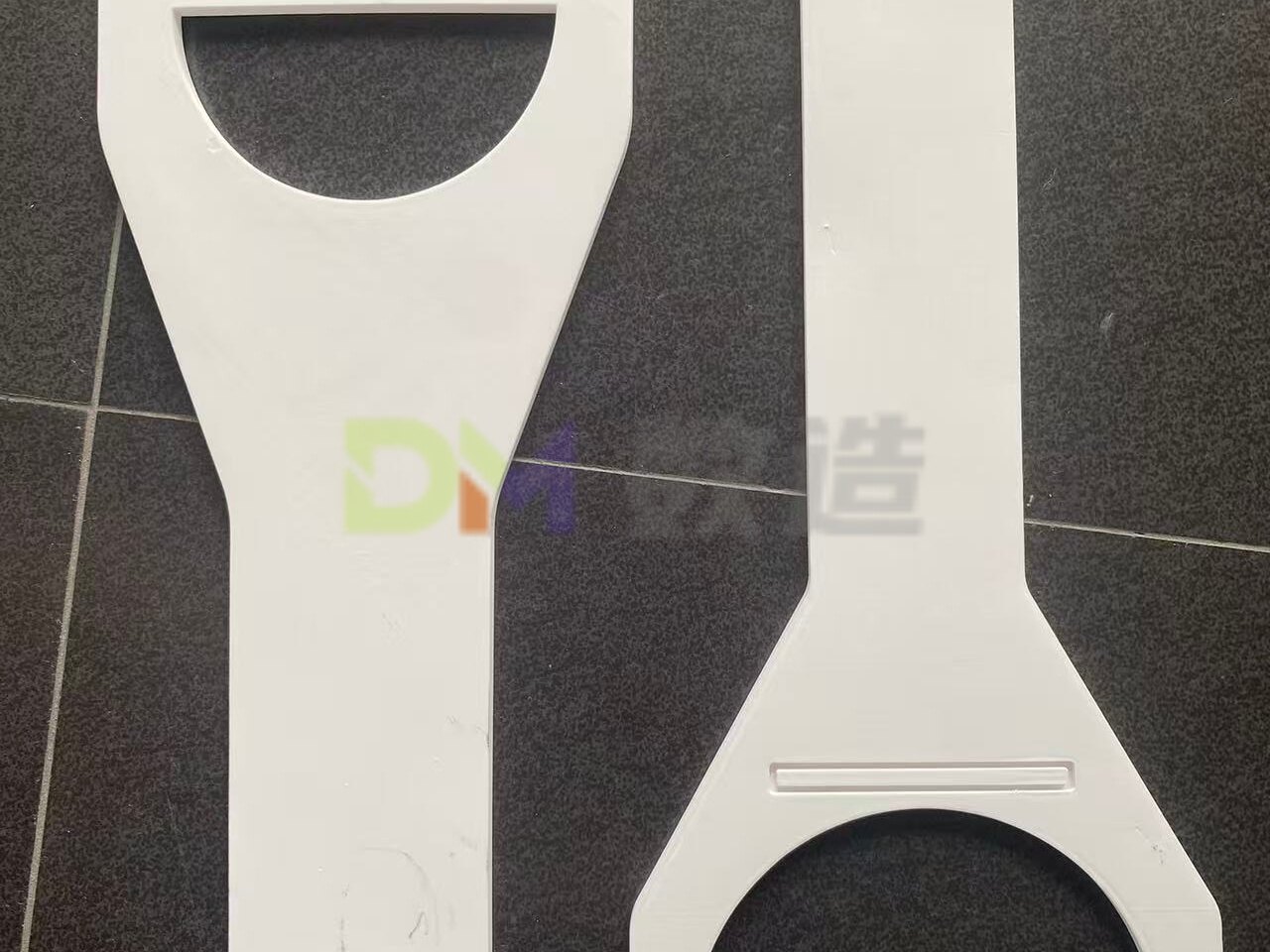
<p>On semiconductor production lines, silicon wafers must be transferred between dozens of processes including lithography, etching, and deposition. Ceramic mechanical fingers are specialized grippers mounted at the end of robotic arms to handle silicon wafers, providing a contamination-free gripping solution.</p> <h3>Why Ceramic?</h3> <p>There are three key reasons:</p> <p><strong>① Zero Contamination</strong>: Ceramic surfaces resist particle shedding, preventing microscopic debris that could scratch wafers or disrupt processes. Metal fingers are a "disaster" in cleanrooms.</p> <p><stron...
On the chip production line, silicon wafers must be transferred between dozens of processes, including lithography, etching, and deposition. Ceramic robotic fingers are specialized grippers mounted at the end of robotic arms to handle silicon wafers, providing a contamination-free clamping method.
Why ceramic?
There are three reasons:
① Zero PollutionCeramic surfaces resist particle shedding to prevent micro-debris from scratching wafers or disrupting processes. Metal fingers are a "disaster" in cleanrooms.
② Ultra-stable: Ceramic materials have an extremely low coefficient of thermal expansion, ensuring consistent clamping force despite temperature fluctuations. They also resist cracking under severe thermal shock.
③ High Precision: The wafer transfer robot arm requires flatness and parallelism errors to be controlled within 0.03mm.
Decisive Advantages of 3D Printing
Unlike traditional manufacturing, 3D printing offers one decisive advantage:Seamless, adhesive-free construction。
Achieving integrated vacuum suction channels in traditional ceramic robotic fingers requires bonding multiple ceramic plates with adhesive before sintering. This approach introduces three critical drawbacks:
- Delamination Risk: The bonded interface is the most vulnerable area; prolonged, high-frequency movement can lead to cracking and delamination.
- Pollution hazard: Adhesive layers can outgas under high-temperature or vacuum conditions, releasing trace contaminants that directly impact wafer yield.
- Precision lossMulti-panel assembly inevitably involves fitment tolerances, making it difficult to ensure overall flatness.
Ceramic 3D printing is entirely different—internal vacuum channels, suction chambers, and positioning structures are all printed in a single piece with no bonded interfaces. Without glue layers, there's no risk of delamination or outgassing contamination. Manufacturing costs are also significantly reduced by eliminating assembly steps.
For chip fabs where yields are measured in parts per ten thousand, this difference isn't a bonus—it's a critical factor directly impacting product yield.
As wafers evolve from 8 inches to 12 inches and even 18 inches, larger finger sizes and more complex structures will further expose the limitations of traditional assembly processes. Meanwhile, the advantages of 3D printing for monolithic manufacturing will become increasingly prominent.
相关文章
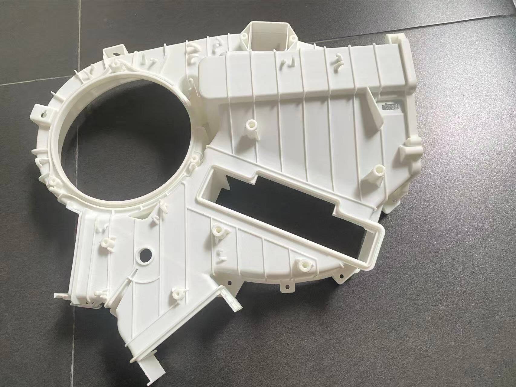
Why Choose SLA 3D Printing for the Four Categories of Prototype Parts in Vehicle R&D?
As the demand for prototype parts in vehicle R&D accelerates, leading automakers are turning to industrial-grade SLA resin 3D printing. With rapid iterations, small batch sizes, and diverse part types, a single machine must cover all three dimensions: build volume, accuracy, and material compatibility. This article breaks down the four most common part categories in R&D prototyping and explains how to configure the right equipment for each.